 Bars
Bars
 Beads & Spheres
 Bolts & Nuts
 Crucibles
 Discs
Discs
 Fibers & Fabrics
 Films
Films
 Flake
Flake
 Foams
Foams
 Foil
Foil
 Granules
 Honeycombs
 Ink
Ink
 Laminate
 Lumps
Lumps
 Meshes
 Metallised Film
 Plate
Plate
 Powders
 Rod
Rod
 Sheets
 Single Crystals
 Sputtering Target
 Tubes
Tubes
 Washer
 Wires
Wires
 Converters & Calculators
 Write for Us
Reshaping Optoelectronic Materials (LiNbO₃, YAG, SOI, Ge) Through Doping Engineering
1 Introduction
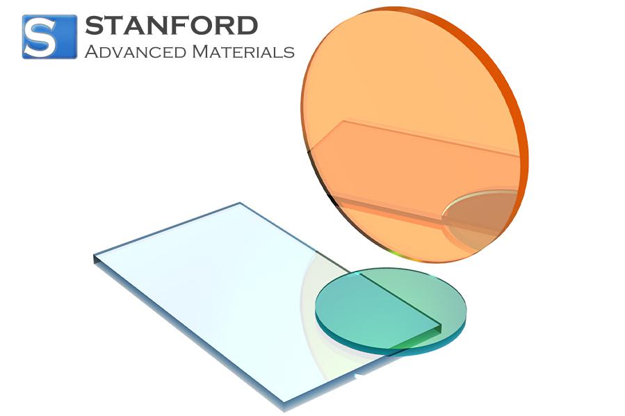
In today's rapidly evolving field of optoelectronics, materials science is undergoing a quiet revolution. By precisely doping key optical materials, engineers are continuously pushing the physical limits of photoconversion efficiency, laser output power, and integration density. While pure crystals possess excellent optical properties, they inevitably have defects in other aspects. The precise method for addressing these defects involves optimizing them through the doping of other ions. Lithium niobate crystals, when doped with rare earth ions, transform from passive materials into gain media for communication-band lasers; and YAG crystals, when doped with neodymium ions, become the core of industrial lasers; and SOI platforms combined with germanium doping technology reduce the dark current of photodetectors by several orders of magnitude. These transformations are quietly reshaping the design blueprint of photonic chips.

Fig. 1 Various Doped Optical Crystals
2 Doped Lithium Niobate
2.1 Properties and Doping Advantages of Lithium Niobate
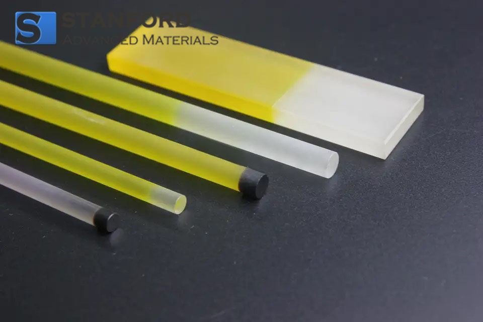
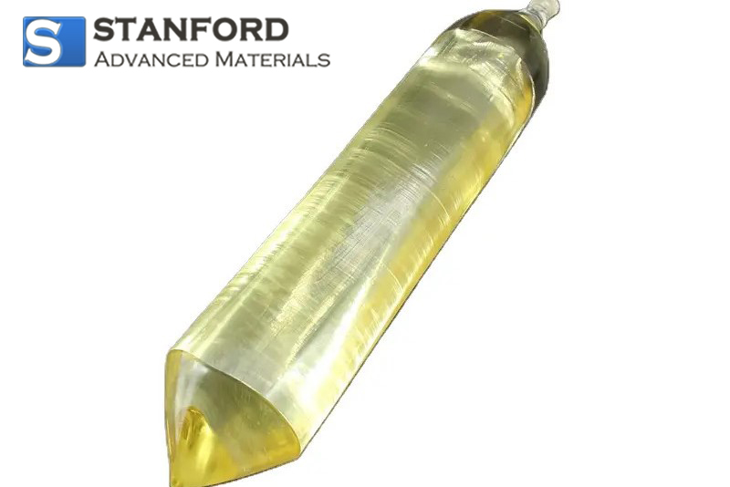
Lithium niobate crystals (LN) are excellent ferroelectric crystals, electro-optic crystals, and nonlinear optical crystals. Pure LN has drawbacks, including susceptibility to light damage and low recording sensitivity, when used as a holographic recording material. To address these issues, doping methods are employed to modify or enhance the properties of LN. The primary dopant transition metals include Fe, Zn, Mn, and Cr, while rare earth elements such as Tm, Er, Eu, and Nd are also commonly used. Mg is frequently employed as a dopant as well. These elements, when doped into LN, can significantly alter its properties. For example, Zn: LN and Mg: LN can enhance LN's resistance to light damage by several orders of magnitude; Fe: LN can improve the recording sensitivity of LN as a holographic recording medium; and MgO: Nd: LN can be used as a laser crystal. Sometimes, to meet multiple usage requirements, dual or multi-doping methods are employed to grow lithium niobate, such as MgO: LN, Fe: MgO: LN, Fe: Nd: LN, Fe: Er: LN, MgO: Nd: LN, and MgO: Er: LN.
Lithium niobate crystals, abbreviated as LN, belong to the trigonal crystal system and have a titanite-type structure. Relative density: 4.30; lattice constants: a = 0.5147 nm, c = 1.3856 nm; melting point: 1240°C; Mohs hardness: 5; refractive indices: n₀ = 2.797, ne = 2.208 (λ = 600 nm); dielectric constants: ε = 44, ε = 29.5, ε = 84, ε = 30; First-order electro-optic coefficients γ13 = γ23 = 10 × 10 m/V, γ33 = 32 × 10 m/V. Γ22 = -γ12 = -γ61 = 6.8 × 10 m/V, nonlinear coefficients d31 = -6.3 × 10 m/V, d22 = +3.6 × 10 m/V, d33 = -47 × 10 m/V. Lithium niobate is a ferroelectric crystal with a Curie point of 1140°C and a spontaneous polarization strength of 50 × 10 C/cm2. Lithium niobate crystals treated with strain exhibit multifunctional properties such as piezoelectricity, ferroelectricity, photovoltaicity, nonlinear optics, and thermoelectricity, while also can exhibit through doping (e.g., Fe) a photochromic effect.

Fig. 2 Doped Lithium Niobate Crystals
2.2 Doping Method
Crystal growth doping method: Rare earth oxides (such as Er2O3) are doped during the pulling method to achieve high doping uniformity, but it is difficult to prepare large-sized crystals. Considering the concentration and uniformity requirements for erbium ion doping, the research team primarily employed thermal diffusion and ion implantation doping methods after two years of continuous experimentation and opted for erbium ion doping during the growth of lithium niobate crystals. The erbium-doped lithium niobate wafers are then processed into silicon-based lithium niobate thin films via ion cutting (smart-cut) technology, addressing future on-chip integration challenges.
Thermal diffusion doping method: After vacuum deposition of a rare earth layer, high-temperature diffusion is applied, suitable for selective doping in localized areas, but concentration uniformity is limited.
Ion implantation doping method: Precisely controls the injection energy and dose, but may introduce lattice damage, requiring post-annealing repair.
2.3 Application Fields
Microcavity laser: Erbium-doped LNOI microdisk cavity (radius 75 μm) achieves laser output in the communication band (~1550 nm) under 974/1460 nm pumping, with a threshold power as low as the μW level, suitable for on-chip coherent communication and quantum light sources.
Heterogeneous integrated amplifiers: Erbium-doped LNOI waveguides integrated with InP/InGaAs avalanche diodes achieve two-stage amplification of optical signals, with a gain increase of over 20 dB.

Fig. 3 Heterogeneous Integrated Amplifiers
3 Doped YAG
3.1 Properties of YAG and Advantages of Doping
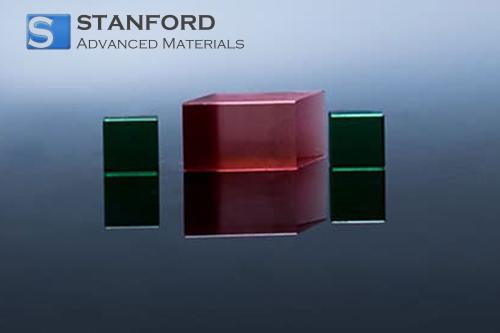
Yttrium aluminum garnet, abbreviated as YAG, is a synthetic crystal of aluminum oxide in which yttrium ions replace some aluminum ions. It is a robust material with excellent hardness, density, and thermal conductivity, making it ideal for high-performance applications. It is renowned for its outstanding thermal, optical, and mechanical properties. These characteristics make it an ideal choice for technological applications such as lasers and optics. This article provides an in-depth comparison between pure YAG crystals and rare-earth-doped YAG crystals.
Rare-earth-doped YAG crystals are essentially YAG crystals impregnated with certain rare-earth elements. The most commonly used elements for doping include neodymium (Nd), erbium (Er), and yttrium (Yb). These elements significantly enhance the performance of YAG crystals in certain applications, particularly in laser technology.
Rare-earth-doped YAG crystals inherit the excellent physical properties of pure YAG crystals, such as high hardness, density, and thermal conductivity. However, the incorporation of rare-earth elements confers unique optical properties on these crystals. For example, they can generate efficient and powerful laser light, a feature highly valued across various industries.
The choice of dopant elements plays a crucial role in defining the characteristics of doped YAG crystals. For instance, neodymium-doped YAG crystals (Nd: YAG) are renowned for their efficiency in generating high-power lasers. On the other hand, erbium-doped YAG crystals (Er: YAG) emit light at wavelengths highly absorbed by water, making them an ideal choice for medical and dental applications.
")
Fig. 4 Neodimium-Doped Yttrium Aluminum Garnet (Nd: YAG)
3.2 YAG Crystal Preparation and Doping Methods
The preparation of pure YAG crystals involves the use of high-temperature, high-pressure technology for artificial synthesis. This process involves the Czochralski method, in which seed crystals are immersed in a molten mixture of yttrium, aluminum, and oxygen. The crystals are then slowly removed, allowing single crystals to form as the molten mixture cools and solidifies. The resulting crystals are carefully cut and polished, ready for use in a variety of applications. Like pure crystals, rare-earth-doped YAG crystals are synthesized using the Czochralski method. However, in this process, specific rare earth elements are introduced into the molten mixture. These elements replace a small portion of the yttrium ions in the crystal structure, forming a doped YAG crystal. The final product not only retains the excellent properties of pure YAG crystals but also exhibits enhanced characteristics due to the presence of the doped elements.

Fig. 5 Czochralski Method
3.3 Typical Doping Systems and Performance
Nd:YAG: The most widely used laser material, with an output wavelength of 1064 nm. When the Nd³⁺ concentration is approximately 1 at.%, it balances high gain with low thermal effects, making it suitable for industrial cutting and medical lasers.
Yb:YAG: Low quantum defect (only 8%) and low thermal load, suitable for high average power lasers (kilowatt-class). The absorption band is at 940 nm, highly compatible with diode pump sources.
Er:YAG: Emits 2940 nm mid-infrared light, strongly absorbed by water molecules, making it an ideal choice for laser medical applications (such as dentistry and dermatology).
Ce:YAG: Converts blue LED light into yellow light, which combines with remaining blue light to form white light, serving as the core fluorescent material for solid-state lighting.
4 Doped SOI
The key difference between SOI (Silicon-on-Insulator) technology and traditional bulk silicon MOS structures lies in the introduction of a buried oxide layer (BOX).
Table 1 Comparison of Different Types of Doped SOI
Device Type | Doped Material | Key Technology | Performance Metrics |
Germanium Photodetector | SiGe Gradient Composition | Crystalline Window Annealing Process | Dark Current Reduction by 10× |
Photon-Integrated Gain Detector | Er:LNOI + InGaAs APD | Flip-chip bonding and CMP thinning | Two-stage gain, bandwidth >40 GHz |
Hybrid Laser | III-V materials + SOI waveguide | Micro-transfer printing technology | Output power >100 mW |

Fig. 6 Structure of SOI Wafer
5 Frontier Applications of Doped Crystals
In today's rapidly evolving field of photonics and quantum technology, three core material systems are reshaping the industry landscape with disruptive innovations: lithium niobate (LN), hailed as the "optical silicon"; yttrium aluminum garnet (YAG), the cornerstone of high-power lasers; and silicon-on-insulator (SOI) platforms, which break through the limitations of silicon-based technologies. The doping techniques and heterogeneous integration solutions for these materials are establishing a comprehensive technological ecosystem spanning applications from quantum communication to industrial lasers.
5.1 Applications of Lithium Niobate
As the ferroelectric crystal with the highest nonlinear optical coefficient, breakthroughs in lithium niobate doping technology are unlocking its full potential. The Er3+-doped lithium niobate thin film (Er: LNOI) microdisk laser developed by the Chinese Academy of Sciences team achieves μW-level threshold power and <1 kHz ultra-narrow linewidth under 1460 nm pumping. These performance metrics make it an ideal light source for quantum precision measurement systems. Even more striking is the electro-pumped hybrid laser scheme—by integrating InP materials with the LNOI platform using micro-transfer printing technology, the output power exceeds the 100mW level, directly meeting the power requirements of 5G base station optical modules and lidar systems.
In the modulator field, the "universal ion knife" technology bonds lithium niobate thin films to SOI wafers, producing electro-optic modulators that support 192 Gbit/s high-speed transmission with excellent low-frequency response flatness. This heterogeneous integration solution not only addresses the fundamental weakness of silicon-based materials in electro-optic effects but also reduces data center optical interconnect energy consumption by 30%. The synergistic design of periodically poled lithium niobate (PPLN) and Er³⁺ has given rise to a dual-wavelength light source: 405 nm violet light for holographic display and 550 nm green light as a quantum bit manipulation light source, demonstrating a new path for material functionalization.
Particularly noteworthy is the femtosecond laser-induced blackening of lithium niobate technology. Through surface micro-nano structuring, this material achieves a two-order-of-magnitude reduction in optical loss and a threefold increase in nonlinear response during ultrafast pulse generation, making it a key component in high-sensitivity detectors and quantum sensing systems.
5.2 Applications of Doped YAG
Yttrium aluminum garnet crystals, with their excellent thermal stability, are breaking through the power limitations of traditional lasers thanks to gradient doping and ion co-doping technologies. The axial concentration gradient Nd: YAG crystals (0.17–0.38 at.%) designed by the Hefei Institute of Physical Science of the Chinese Academy of Sciences achieve a 42% increase in thermal lens focal length and reduce thermal stress to 60% of that in traditional structures by precisely controlling the dopant concentration distribution. Under 808 nm pumping, the system maintains linear power growth at 110 W output power, with a light-to-light efficiency of 51.9%, a figure approaching the theoretical limit of laser media.
A more groundbreaking advancement is seen in the Q-switched laser design: the optimized single-rod Nd: YAG system outputs 12W at 1064nm laser at a 2kHz frequency, with a peak power of 882kW, a beam quality M2 < 1.25, and a brightness metric of 5.02 × 10^13W/(cm2·Sr), setting a new record for similar devices. This high-brightness light source is revolutionizing the rules of the game in precision processing and medical surgery—in femtosecond laser microprocessing, its focused spot diameter can be compressed to below 5 μm; in ophthalmic surgery, it enables precise cutting without thermal damage.
In the field of luminescent materials, (Gd, Lu)3Al5O12:Tb3+/Eu3+ transparent ceramics achieve green-to-red emission switching through energy transfer mechanisms, with a 30% increase in quantum efficiency. This tunable material has achieved 95% NTSC color gamut coverage in micro-projection, while the radiation-resistant properties of Ce3+-doped YAG ceramics make them a critical component in spacecraft onboard processors, with a single-particle flip rate reduced by 87.5% compared to traditional devices.
5.3 Applications of Doped SOI Materials
Silicon-on-insulator (SOI) technology, through germanium doping and heterointegration, is breaking through the bandgap limitations of silicon materials. In the field of photodetectors, SiGe gradient doping technology combined with a silicon nitride barrier layer has improved the quantum efficiency in the 1310/1550 nm wavelength band to over 90% and reduced dark current to the 0.1 nA level. Black silicon detectors prepared using femtosecond laser supersaturated doping have sulfur/selenium doping concentrations exceeding 10¹⁹ cm-3, with a spectral response range extended to 400–1700 nm. These flexible devices have completed field testing in unmanned aerial vehicle (UAV) optoelectronic systems.
At the forefront of integrated photonics, wafer-level bonded lithium niobate-SOI electro-optic modulators demonstrate a modulation bandwidth of 40 GHz, with power consumption reduced by 30% compared to traditional solutions, perfectly suited for 5G/6G millimeter-wave communication requirements. Of particular note is the photonic integrated gain detector: the monolithic integration of erbium-doped LNOI amplifiers (gain > 20 dB) with InGaAs avalanche diodes has pushed optical communication receiver sensitivity beyond -30 dBm. This technology has been validated through 1,000-kilometer relay-free transmission in submarine cable systems.

Fig. 7 Applications of Silicon-Based Photonic Integration in The Telecommunications Field
6 Future Outlook: Material Synergy and System Integration
The breakthroughs in these three material systems are not isolated developments but exhibit significant synergistic effects. The combination of lithium niobate's high nonlinearity and SOI's CMOS compatibility is giving rise to ultra-low-loss photonic integrated circuits. Meanwhile, the high-power characteristics of YAG combined with lithium niobate's electro-optic modulation may lead to the development of a new generation of lidar transmitter modules. As wafer-level hybrid integration technology matures, photonic chips are evolving from discrete components to multifunctional systems—from quantum key distribution to artificial intelligence optical computing, from industrial laser processing to biomedical imaging. This materials revolution is redefining the boundaries of photonic technology.
The journey of these advanced materials from research to real-world application relies on a robust supply chain for high-quality substrates and wafers. At Stanford Advanced Materials (SAM), we provide the foundational materials—including high-purity lithium niobate and YAG crystals, as well as specialized SOI wafers—that enable the innovations in lasers, modulators, and photonic integration discussed throughout this article. We are committed to supporting researchers and engineers in transforming the design blueprint of photonic chips into commercial reality.

 Dr. Samuel R. Matthews